Lab/Tutorial 2 - Introduction to Cadence Layout Design
In this lab, you will be using Cadence to design an inverter at both the schematic
level using transistors and at the layout level. You will be using a similar process
in the remaining labs to design various circuits and components at the layout level.
Inverter Layout Library
- From now on, you should create all of your designs using the NCSU_TechLib_hp06 process technology files,
prepared at North Carolina State University.
- As recommended, you should create a library for your inverter design.
- Using the Library Manager Window, select File => New => Library.
- Enter the library name mylib_inverter in the Name field.
- Enter the path ~ in the Path field.
- Select the option Attach existing tech library under Technology Library.
- You library creation should look similar to the following.
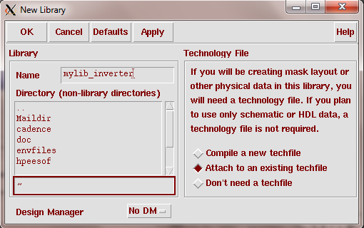
- Click OK.
- Select the NCSU_TechLib_hp06 library, then click OK.
Inverter Layout Tutorial
The design of the inverter will follow the tutorial available at
Cadence Tutorial. Please follow
this tutorial keeping in mind the following changes and additional steps that must be
followed.
- Your inverter cell name should be my_inverter(schematic, symbol, layout).
- Your test circuit cell name should be my_inverter_test(schematic).
- In designing the schematic and layout of your inverter, the width should be
1200n m and the length should be 600n m.
- Within the tutorial, when you get to the Mask Layout step, follow the
Manual Layout Example.
- If you can't draw P and N Substrate contact when following the tutorial, draw it manually.
- Within the tutorial, you can skip the LVS step.
Inverter Layout Pins
The provided tutorial does not discuss the steps required to add pins
to the layout design that are neccesary. After creating your inverter layout
but before extraction, you must add pins to your layout corresponding with
the pin you created in your schematic design. The following is a simple
description of how to add those pins.
- Within the Layout Editing window, Select Create => Pin. You should be
be presented with the following window.
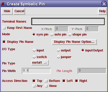
- First ensure the Mode is set to sym pin.
- Enable the option Display Pin Name.
- Select the Pin Type as metal1.
- You now need to add four pins to the design, vdd!, gnd!, Inp, Outp using the
following specification for each pin. After entering the proper information,
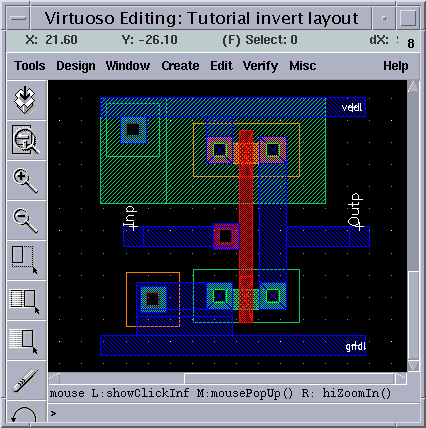
you can add the pin to your layout by swicthing to the Layout Editing window
and adding the pins in the proper locations as shown here.
- Terminal Name: vdd!, IO Type: InputOutput, Access Direction: Top, Left, Right.
- Terminal Name: gnd!, IO Type: InputOutput, Access Direction: Bottom, Left, Right.
- Terminal Name: Inp, IO Type: Input, Access Direction: Top, Bottom.
- Terminal Name: Outp, IO Type: Output, Access Direction: Top, Bottom.
Inverter Layout Simulation
After properly extracting your layout design, you can use your test circuit to simulate the
extracted circuit. Please make sure you do not skip the Simulating the Extracted Cell View
step. During this step you will indicate to the simulator that you want to simulate the
extracted layout instead of the schematic design.
Demo
You must demo the following aspects or your NAND gate design to the TA.
- Inverter schematic design and simulation.
- Inverter layout design and extracted layout simulation.
Lab Report
In addition to the standard lab report format, you must submit the following information.
- Inverter schematic.
- Inverter test circuit schematic.
- Inverter layout.
- Inverter schematic and extracted layout simulations.